AEMD currently operates two cleanroom facilities located in the East and West Areas, with a total cleanroom area of approximately 1,800 m² and equipment assets exceeding RMB 300 million. The platform has established both 6-inch and 8-inch semiconductor-grade pilot fabrication lines, offering a complete process chain covering: Thin-film deposition and growth, Photolithography, Dry etching, Wet cleaning and wet etching, Packaging, Characterization and testing. AEMD is equipped with advanced micro/nanofabrication and testing instruments, including: KrF deep ultraviolet stepper lithography (150 nm), Electron beam direct writing (10 nm), Focused ion beam dual-beam systems, Nanoimprint lithography, Maskless laser direct writing, Ion implantation, Molecular beam epitaxy (MBE) for semiconductor materials. The platform supports fabrication from sub-10 nm scale up to micrometer scale. AEMD can process and support the development of advanced micro/nano devices in multiple fields, including: Optoelectronic devices, Emerging memory devices, MEMS (Micro-Electro-Mechanical Systems), Biochips, Microfluidics.
AEMD follows the SIIS management philosophy: Service · Interaction · Innovation · Satisfaction. The platform supports research in a wide range of disciplines, including: Electronics, Physics, Mechanical Engineering, Materials Science, Optics, Chemistry, Instrumentation, Environmental Science, Medicine, Biology. In addition to supporting internal interdisciplinary research at Shanghai Jiao Tong University, the platform is also open to external universities, research institutes, and industrial users. AEMD provides micro/nanofabrication services for silicon-based, glass-based, and polymer-based devices and structures using 6–8 inch wafers and smaller compatible sizes. It also offers technical support and collaborative R&D services for scientific projects and emerging products, actively promoting the industrialization of micro/nano technologies in China.
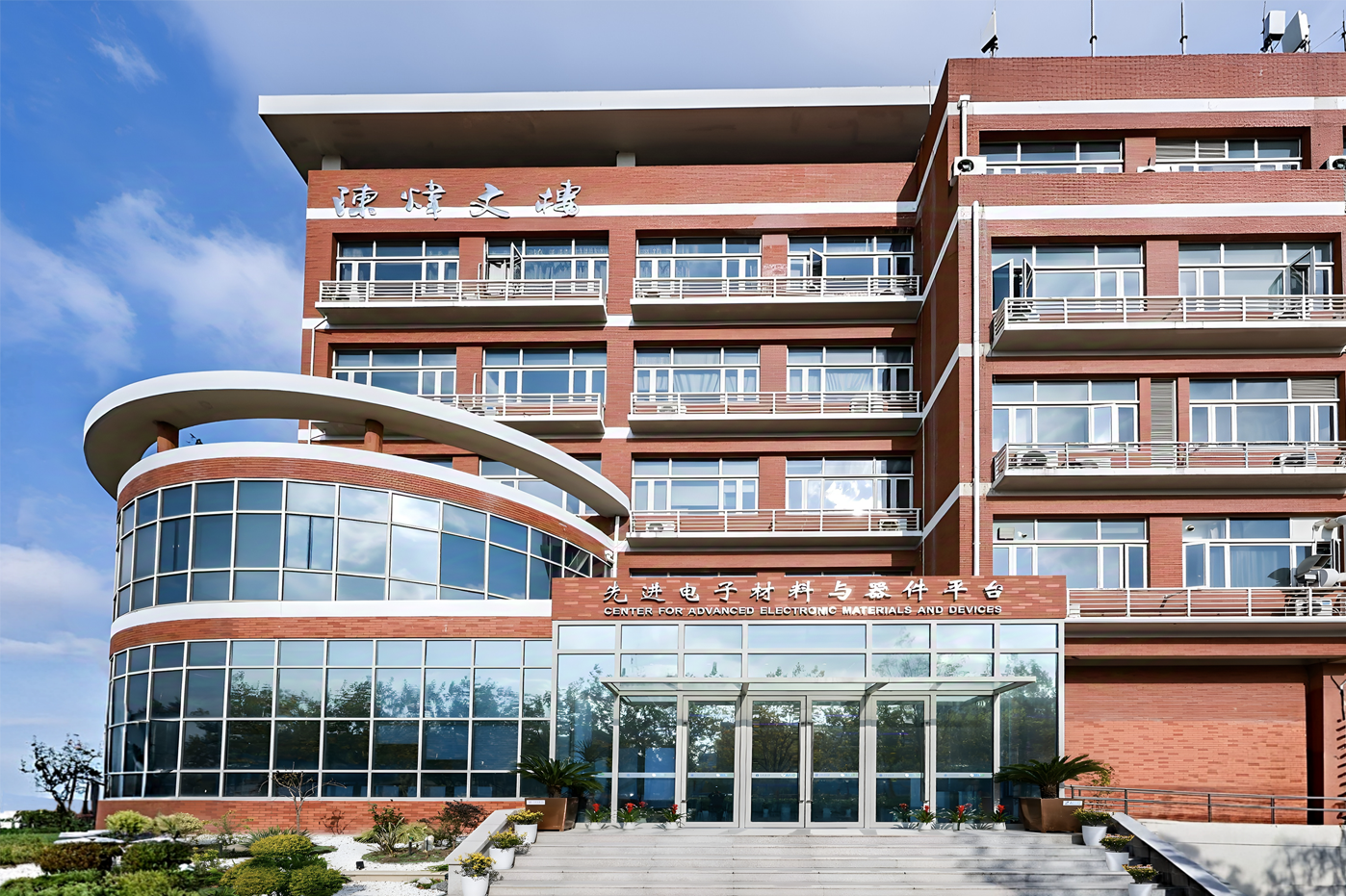


Address: 800 Dongchuan Road, Minhang District, Shanghai 200240, China
Tel: +86 21 3420 7734
Email: [email protected]







