Patterning
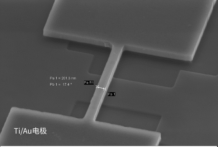
EBL + electron beam evaporation for fabrication of Ti/Au metal electrodes with 200 nm linewidths based on a lift-off process:


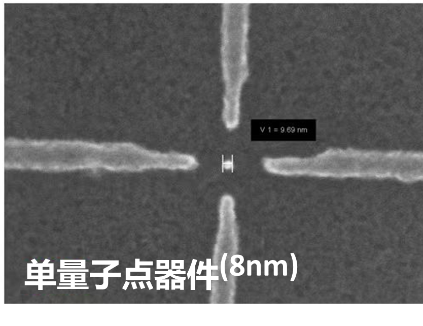
00KV Electron Beam Lithography (EBL): Min. 8~10 nm

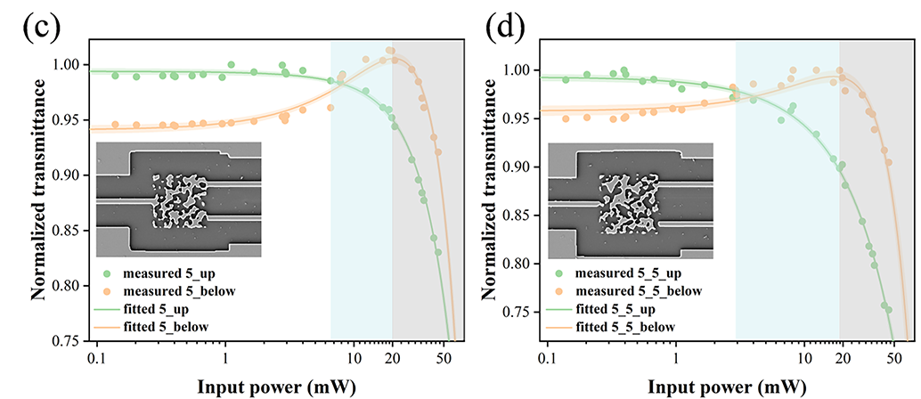
Nonlinear activator for optical computing.

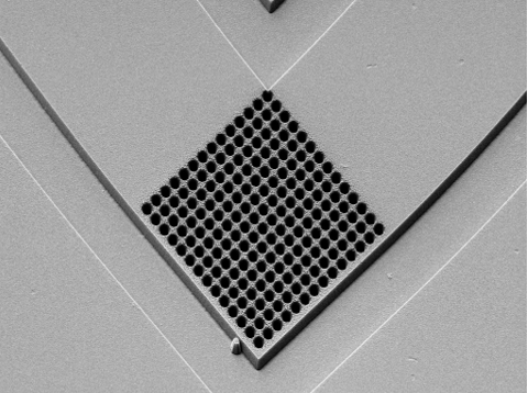
EBL+ICPRIE:minimum designed feature size of 100 nm and etch depth of 220 nm.
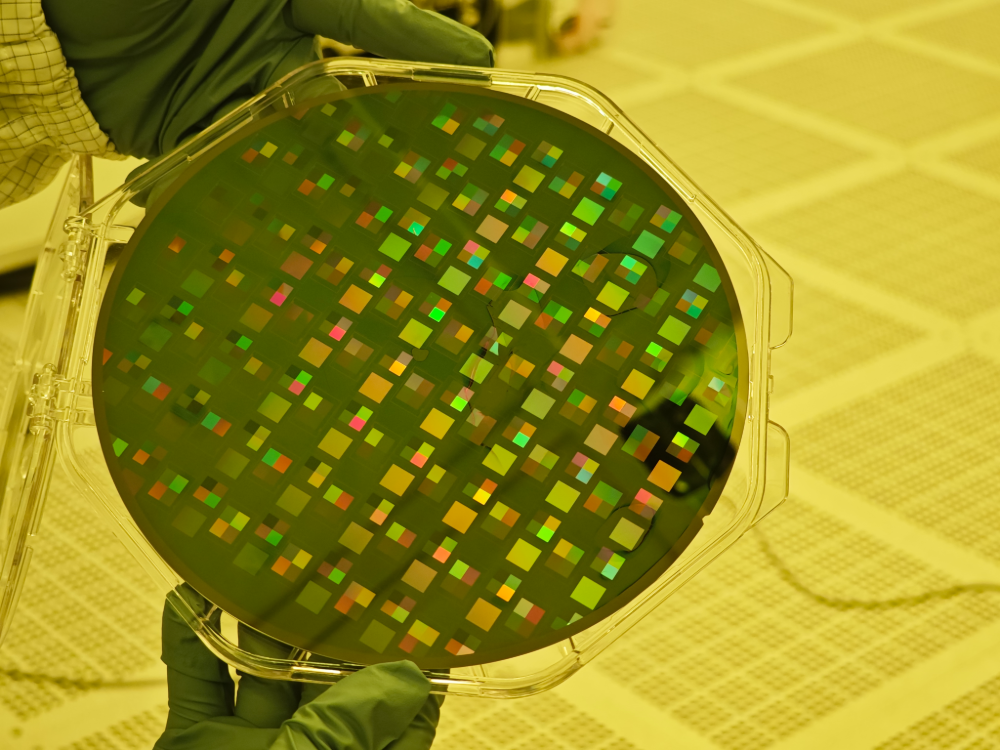
 

Patterned 8-inch wafer after DUV lithography.Photoresist thickness: 400 nm; minimum feature size: 200 nm.


3D micro/nano printing of enclosed microfluidic channels:Min. 100 nm


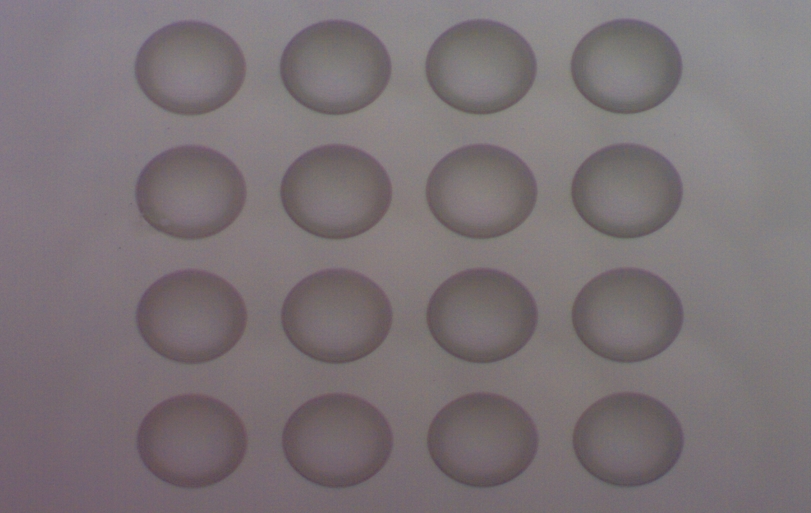
Laser maskless direct-write grayscale lithographyThe current minimum resolution of the system is 0.6 μm.


Nanoimprint Lithography (NIL): Min. ≤20nm
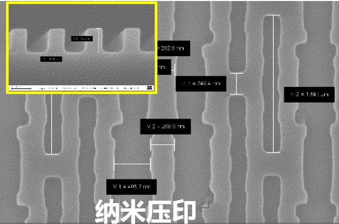
 

Focused Ion Beam (FIB) direct deposition and etching: Min. ≤20nm

×