Platform History

The Advanced Electronic Materials and Devices (AEMD) University-Level Platform was founded in 2012 and officially began external operation on November 6, 2014. It serves as a university-level shared instrumentation platform supporting scientific research across the university, with fabrication and testing capabilities ranging from 10 nm to the micrometer scale. With strong support from university leadership at all levels, AEMD has become an important infrastructure platform supporting multiple disciplines while providing comprehensive technical support for research activities.
  • 2020-2024
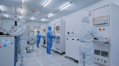
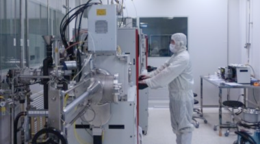
    Phase II and Phase III Cleanroom Expansion
    Supported by the university’s Double First-Class construction initiative, a new cleanroom facility of nearly 1,200 m² was completed in the Comprehensive Laboratory Building. New equipment with a total value exceeding RMB 230 million is being progressively opened for full operation. The Phase II and III expansion significantly enhances AEMD’s support capabilities in areas such as: Optoelectronic semiconductor devices,3D heterogeneous integration and packaging,MEMS and micro/nano sensing systems,Micro/nano optics. This expansion addresses critical research support needs at Shanghai Jiao Tong University in: Semiconductor processing, Integrated circuits, Photonic chips, Micro/nano sensing technologies.
  • 2014-2020
    Stable Operation of the Phase I Cleanroom
    In November 2014, AEMD officially opened its facilities to internal and external users. During this period, the platform became one of China’s leading open-access micro/nanofabrication facilities, known for its high degree of openness and efficient operation. To date, AEMD has supported: 2,550 internal users, 20 internal schools, departments, and research institutes; 53 domestic universities, 23 research institutes, including 13 institutes of the Chinese Academy of Sciences, 95 industrial enterprises. Its user base now spans across China.
  • 2011-2014
    Phase I Construction and Initial Operation
    Supported by the university’s “985 Project” Phase III key initiatives, AEMD completed its first cleanroom facility with a total area of 618 m². During this stage, the platform established: a 6-inch semiconductor-grade micro/nanofabrication line compatible with silicon, glass, and organic substrates, a 3-inch non-silicon micro/nanofabrication line, an optoelectronic materials and devices laboratory. The platform achieved minimum feature sizes of better than 8 nm. The total value of process and testing equipment at this stage exceeded RMB 93 million. Its process capabilities covered: Photolithography, Oxidation and diffusion, Wet cleaning and wet etching, Physical vapor deposition (PVD), Chemical vapor deposition (CVD), Dry etching,Structural and device characterization.  Advanced capabilities also included: Electron beam lithography, Focused ion beam deposition and processing, Deep silicon etching.
×