| Model: | SE-2000 |
|---|---|
| Function: | It is used to detect the refractive index (n), extinction coefficient (k), thickness and other parameters of single-layer or multilayer thin films. |
| Engineer: | Qu / +86-21- 34207734-8003 / minni.qu@1 |
| Location: | West Area – Testing I |
| Equipment ID: | WT1SELP01 |
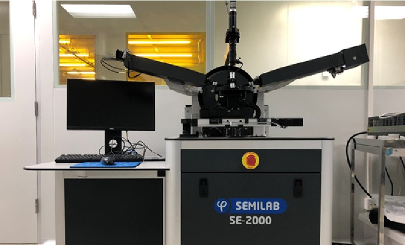
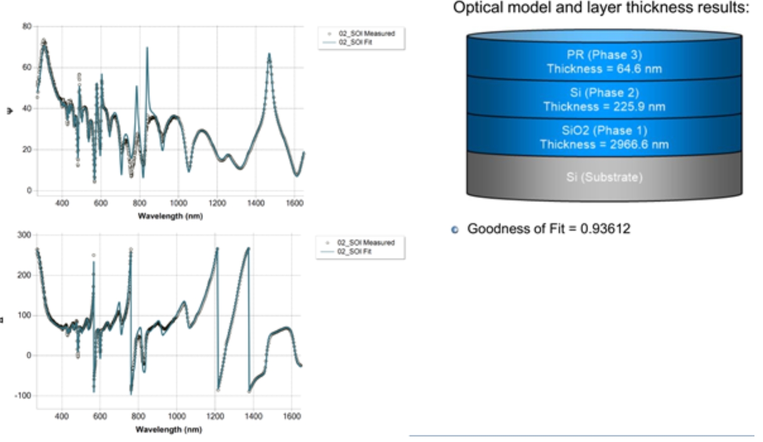
The instrument provides spectroscopic ellipsometry measurement in the ultraviolet-visible-near infrared (245 nm~1600 nm) wavelength range, and can characterize the refractive index (n), extinction coefficient (k), thickness and other parameters of single-layer and multilayer thin films. Adopting an optical reflection mode, the measurement is non-destructive and efficient.It is applicable to thin film characterization of semiconductor materials including silicon oxide, silicon nitride, silicon oxynitride, high-k dielectric materials (such as HfO₂), low-k materials, photoresist, SOI, SiGe, SiC, polysilicon and strained silicon; IGZO and electrochromic layers for flat panel displays; as well as ferroelectric materials. It also supports compound semiconductor materials for optoelectronic devices such as AlGaN, GaN and InP; transparent conductive thin films and nanomaterials for solar cells; and organic thin films used in OLED and OTFT devices.For ultra-thin film measurement, it is suitable for ultra-thin dielectric films grown by atomic layer deposition (ALD), as well as emerging two-dimensional materials such as monolayer graphene. Meanwhile, the equipment is equipped with a non-contact eddy current measurement module, enabling non-destructive and rapid sheet resistance testing for conductive and semiconductor thin layers.
Process/Testing Capabilities
Wavelength measurement range: 245 nm ~ 1600 nm.For 120 nm-thick SiO₂/Si standard samples:Measurement accuracy of thickness ≤ ±5 Å;Thickness repeatability ≤ 0.2 Å;Refractive index accuracy ≤ ±0.009;Refractive index repeatability ≤ 0.002;1σ repeatability of extinction coefficient ≤ 2%.For sheet resistance measurement with 10 repeated tests, the 1σ repeatability is less than 3%.
Technical Specifications

Address: 800 Dongchuan Road, Minhang District, Shanghai 200240, China
Tel: +86 21 3420 7734
Email: [email protected]







