| Model: | ULTRA PLUS |
|---|---|
| Function: | High-resolution microscopic morphology observation and micro-area compositional analysis. |
| Engineer: | Wang / +86-21- 34207734-8006 / wangying@1 |
| Location: | West Area – Testing II |
| Equipment ID: | WT2ZSEM01 |
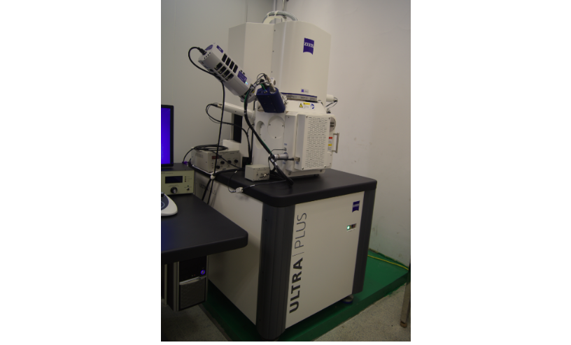
It is primarily used for ultra-high-resolution microscopic morphology observation of micro- and nano-scale materials and structures. It can also be combined with an energy-dispersive X-ray spectroscopy (EDS) system to perform micro-area compositional analysis of material or structure surfaces and cross-sections.
Process/Testing Capabilities
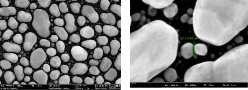
Field emission scanning electron microscopy (FE-SEM) is widely used in the inspection of semiconductors, inorganic non-metallic materials, and devices due to its high resolution, large depth of field, enhanced stereoscopic imaging, and wide adjustable magnification range.
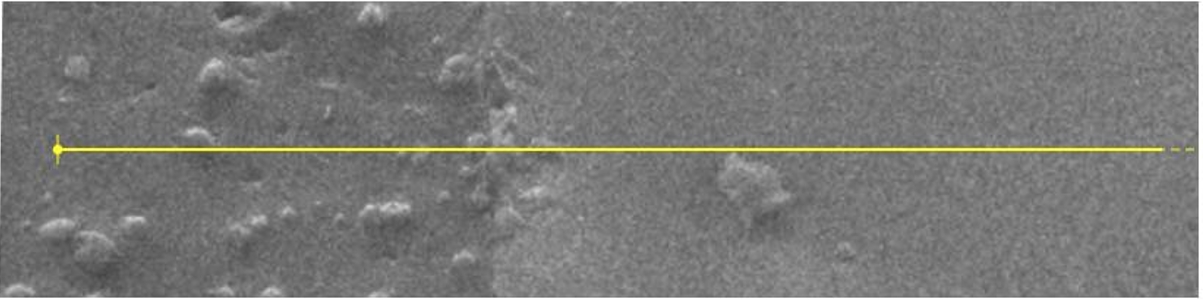
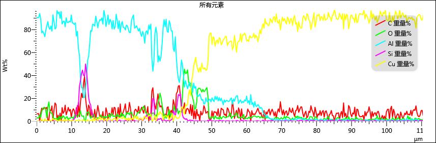
It enables secondary electron imaging and backscattered electron imaging of surface morphology for various solid samples, as well as image processing. When equipped with an energy-dispersive X-ray spectroscopy (EDS) system, it can perform qualitative, semi-quantitative, and quantitative elemental analysis at micro-regions (point, line, and area) on the sample surface. It provides integrated analytical capabilities for both morphology and chemical composition.
Technical Specifications
1. Resolution: ≤ 0.8 nm @ 15 V; ≤ 1.6 nm @ 1 kV
2. Accelerating voltage: 0.02 kV–30 kV; excellent low-voltage performance suitable for observing low-conductivity samples
3. Detectors: in-lens high-efficiency secondary electron detector and energy-selective backscattered electron detector; chamber-mounted high-efficiency secondary electron detector and angle-selective backscattered electron detector, enabling simultaneous acquisition of SE and BSE images
4. Sample stage: maximum sample size Φ200 mm
5. Five-axis motorized eucentric stage, tilt range -3° to 70°, continuous 360° rotation
6. Equipped with EDS system for micro-area compositional analysis
7. Ion sputter coater for gold (Au) coating deposition
When equipped with an energy-dispersive X-ray spectroscopy (EDS) system, it allows simultaneous microscopic morphology observation and micro-area compositional analysis.
1.The sample must be a dry, anhydrous solid with no volatile solvents.
2.Non-magnetic materials only.
3.Porous materials must be pre-vacuumed prior to operation.Self-service operating hours:11:30–13:30 (noon) and 17:00–22:00 daily.
A. Point analysis selects a small region on the sample for measurement, providing information such as elemental species and relative composition.
B. Line scan performs continuous measurements along a line to obtain compositional variation along that line.
C. Area mapping scans a selected surface region to acquire elemental distribution information across the entire area.
B. Mount the sample vertically on the sample holder, with the cross-section surface facing upward for observation.
B. The sample surface should have good electrical conductivity; if conductivity is poor, gold or carbon coating can be applied to improve it.
C. The sample must not contain volatile substances.
D. The sample should be resistant to electron beam damage.

Address: 800 Dongchuan Road, Minhang District, Shanghai 200240, China
Tel: +86 21 3420 7734
Email: [email protected]







