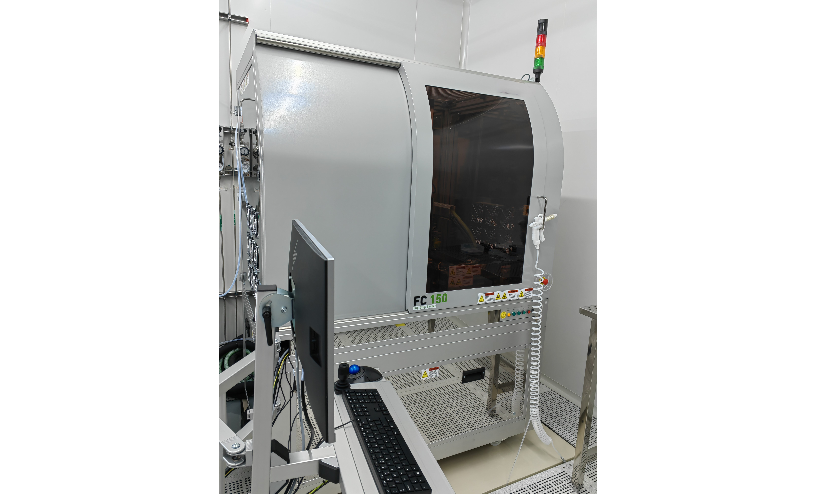
High-Force Chip Bonder
FLIP-CHIP BONDER
Operating
Model: 150
Function: Supports cold pressing, thermocompression reflow and eutectic processes for various types of chips. The equipment is capable of flip-chip bonding and face-up bonding, enabling bonding modes such as chip-to-chip and chip-to-wafer.
Engineer: Liu / +86-21-34206126-6027 / liudanqh@1
Location: East Area – Packaging II
Equipment ID: EPK2FCB01
  • Basic Equipment Information
  • Operating Principle
  • Typical Application Case
Main Application

The high-force chip bonder features precise parallelism adjustment capability for chips, high bonding pressure and superior bonding accuracy, enabling its extensive applications in the assembly of optoelectronic and photonic devices, focal plane devices, 3D integration and other related fields.


Process / Testing Capabilities

  • The high-force chip bonder supports cold pressing, thermocompression reflow and eutectic processes for various chips;
  • The equipment is equipped with flip-chip and face-up bonding functions, and can realize bonding modes such as chip-to-chip and chip-to-wafer.


Technical Specifications

  • Interconnection accuracy: ±1–3 μm;
  • Bonding pressure: 0.6~2000N, resolution: 0.06N–2N;
  • Temperature control range: Room temperature to 450 ℃ (bond arm); Room temperature to 350 ℃ (stage); resolution: 1 ℃;
  • Chip size: 2×2 mm – 50×50 mm (bond arm), 2×2 mm – φ200 mm (stage)
Flip-chip bonding technology mounts chips face-down and interconnects them to substrates, wafers or circuit boards via bumps, forming stable and reliable mechanical and electrical connections.The equipment performs leveling, alignment and bonding of chips, and enables interconnection between chip bumps and packaging substrates through soldering, thermocompression and other processes with the chip electrode side facing downward.
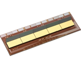
Focal Plane Array(Image sourced from the official promotional picture on the equipment website)

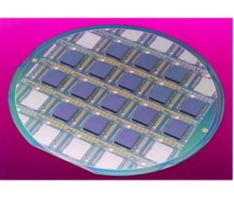
Image Sensor(Image sourced from official promotional material on the equipment website)

Radio Frequency Field(Image sourced from official promotional picture of the equipment website)

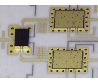
Radio Frequency Device(Image sourced from promotional materials on the equipment official website)
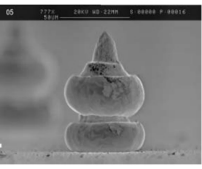

Both the front and back sides of the sample shall be kept clean, and in particular, the back side must be free of contamination and particulate matter.
The list below shows FAQs (click a question to view the answer). If your question is not listed, you can leave a message using the link.
FAQs
  • 01
    How to perform leveling if the sample surface flatness is unsatisfactory?
    It is required to pre-fabricate three reflective layer regions on the sample with a size of no less than 50×50 μm (generally metal layers such as Cr layer).
Message Inquiry
If your question is not listed above, please email us at [email protected] or click the button below to submit an inquiry.
Note: "@1" represents "@sjtu.edu.cn"
×