| Model: | 500TC |
|---|---|
| Function: | 1. Substrate thin film stress measurement (Note: Measurement is required once before and once after thin film deposition);2. Thin film stress measurement with temperature rising from room temperature to 500℃. |
| Engineer: | Liu / +86-21- 34206126-6013 / minliu@1 |
| Location: | West Area – Thin Film II |
| Equipment ID: | WF2FSTR01 |
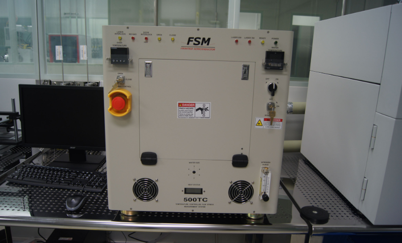
The thin film stress tester adopts a non-contact laser scanning method to measure the curvature change of wafers before and after coating, and calculates the thin film stress by the Stoney formula. It is mainly used for stress detection of semiconductor thin films.
Process/Testing Capabilities
The thin film stress is calculated by measuring the curvature change of the substrate before and after thin film deposition.
Technical Specifications
Only intact wafers of 8 inches and below are accepted, with reflective sample surface required.
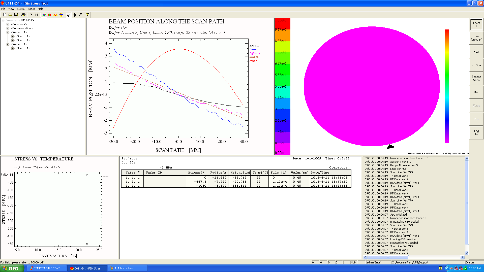
Temperature rise measurement shall be specified in advance.

Address: 800 Dongchuan Road, Minhang District, Shanghai 200240, China
Tel: +86 21 3420 7734
Email: [email protected]







