| Model: | F50-UVX |
|---|---|
| Function: | Thin film thickness measurement with automatic mapping function. |
| Engineer: | Fu / +86-21- 34206126-6010 / xuecheng.f@1 |
| Location: | West Area – Thin Film IA |
| Equipment ID: | WF1TFMF01 |
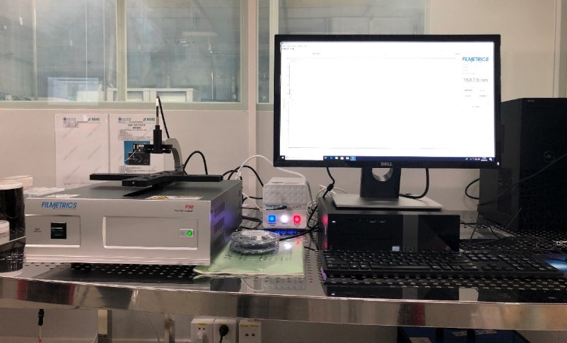
It enables non-contact and non-destructive thickness measurement of thin film samples, capable of testing thin film thickness and optical constants. It features fast measurement and simple operation, with accuracy typically reaching the nanometer or angstrom level. The wavelength range is selectable from ultraviolet to near-infrared. The sample stage supports 12-inch and smaller wafers, including irregular fragments, and supports automatic area scanning. It is widely used to measure the thin film thickness of various materials such as silicon dioxide, silicon nitride, silicon, and photoresist.
Process/Testing Capabilities
It is applicable to the non-destructive measurement of thin film thickness for various materials such as silicon dioxide, silicon nitride, silicon and photoresist. It is widely used in various fields ranging from basic research to industrial production, including semiconductor materials, thin film growth, and lithography process monitoring.
Technical Specifications
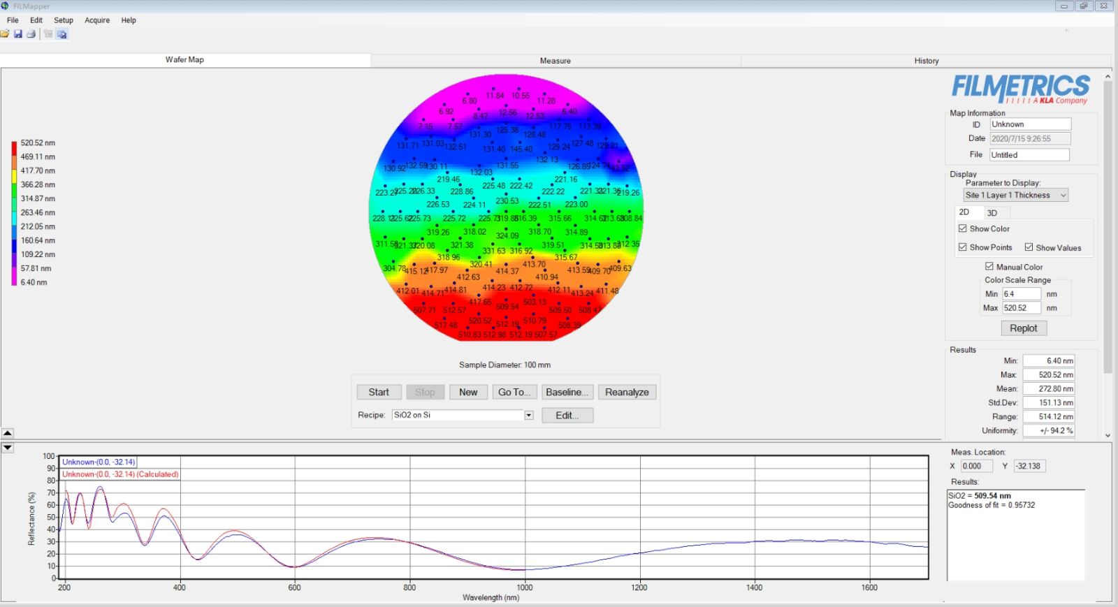
Turn off all light sources after measurement is completed.
Solution: Check the indicator light status of the baffle and light source switch buttons. The indicator stays steadily on when normally turned on. Contact the process engineer in case of any abnormality.

Address: 800 Dongchuan Road, Minhang District, Shanghai 200240, China
Tel: +86 21 3420 7734
Email: [email protected]







