| Model: | CVP21 |
|---|---|
| Function: | Measurement of depth-dependent doping concentration distribution on silicon wafer surface, with the carrier concentration ranging from 10¹¹ cm⁻³ to 10²¹ cm⁻³. |
| Engineer: | Li / +86-21- 34206126-6012 / litq@1 |
| Location: | East Area – CMP |
| Equipment ID: | ECMPECV01 |
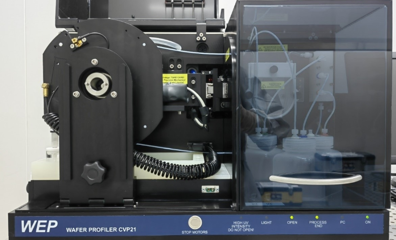
Electrochemical CV measurement is mainly applied to the research and development of semiconductor materials. Its principle adopts the electrochemical capacitance-voltage (C-V) method to measure the doping concentration distribution of semiconductor materials. A suitable electrolyte is selected to make contact with and etch the material. Through C-V scanning, the doping concentration distribution on the surface of silicon substrates can be accurately measured, which is used to evaluate and control the doping process in semiconductor manufacturing. The measurable carrier concentration ranges from 10¹¹ cm⁻³ to 10²¹ cm⁻³.
Process/Testing Capabilities
It can rapidly measure and calculate the sheet resistance, junction depth and surface concentration of the diffusion layer, and is suitable for evaluating and controlling the epitaxial process in semiconductor manufacturing.
Technical Specifications
Maximum sample size: 8-inch wafer.The minimum sample size shall cover the sealing ring area and make contact with two probes simultaneously; a size of 2 cm×2 cm or larger is recommended.
The carrier concentration ranges from 10¹¹ cm⁻³ to 10²¹ cm⁻³.
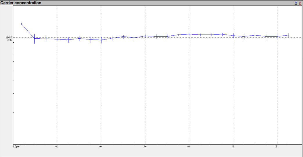
1. It is required to scrape both ends of the sample surface to form contact points for probes.
2. The tested area will be etched by corrosive solution.

Address: 800 Dongchuan Road, Minhang District, Shanghai 200240, China
Tel: +86 21 3420 7734
Email: [email protected]







