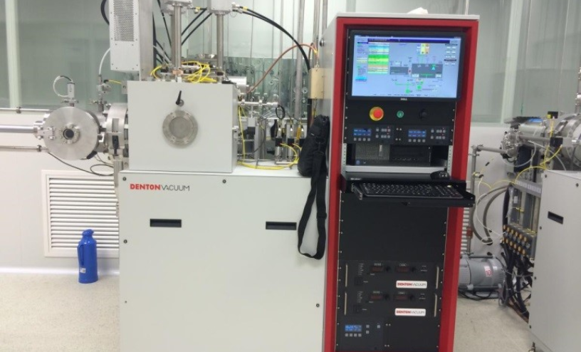
| Model: | Explorer-14 |
|---|---|
| Function: | Used for the sputtering deposition of various metal thin films;Reactive sputtering deposition of multiple oxide and nitride thin films; Equipped with the function of in-situ substrate cleaning. |
| Engineer: | Fu / +86-21- 34206126-6010 / xuecheng.f@1 |
| Location: | West Area – Thin Film IA |
| Equipment ID: | WF1DMSP01 |
Process/Testing Capability
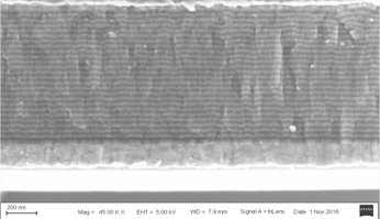
Capable of sputtering a variety of metal, semiconductor and ceramic thin films with controllable thickness, including Cr, Cu, Ag, Al, Ti, Mo, ITO, AZO, TiNx, etc.
The maximum deposition thickness is generally no more than 3 μm. The resistivity of deposited metal thin films can be adjusted on demand.
Technical Specifications
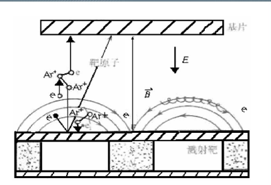
High-energy particles with energy exceeding the sputtering threshold bombard the target surface, ejecting target atoms. These atoms deposit onto the substrate to realize sputtering coating.

Address: 800 Dongchuan Road, Minhang District, Shanghai 200240, China
Tel: +86 21 3420 7734
Email: [email protected]







