| Model: | E550D |
|---|---|
| Function: | Capable of depositing high-quality thin films with precisely controllable thickness at room temperature, including elemental metals (especially refractory precious metals such as Pt and Pd) and various compound materials. |
| Engineer: | Fu / +86-21- 34206126-6010 / xuecheng.f@1 |
| Location: | East Area – Thin Film IV |
| Equipment ID: | EFM3EBE01 |
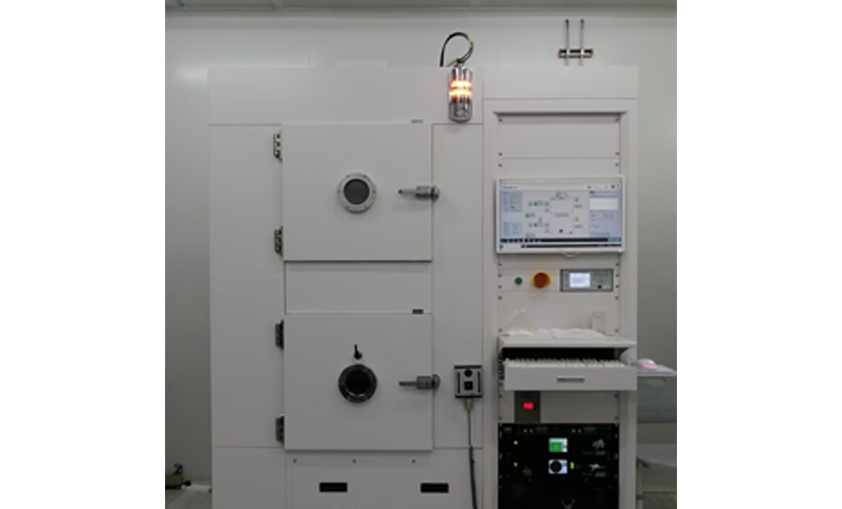
At room temperature, metal thin films such as Cr, Cu, Ni, Al, Y, Ti, Pt and Pd can be deposited by evaporation on samples smaller than 8 inches, fully meeting the requirements of the lift-off process.
Process/Testing Capability
1. Supports thin film evaporation for samples up to 8 inches in size;
2. Capable of depositing metal thin films including Cr, Cu, Ni, Al, Y, Ti, Pt and Pd;
3. Enables film deposition at room temperature for evaporation with photoresist retained.
Technical Specifications
1. Non-uniformity: ±5% @ 8-inch substrate;
2. The thickness of evaporated aluminum films is limited to 1 μm maximum;
3. For materials with an obvious hollowing effect during evaporation (e.g., Cr), the non-uniformity is ±10% @ 8-inch substrate.
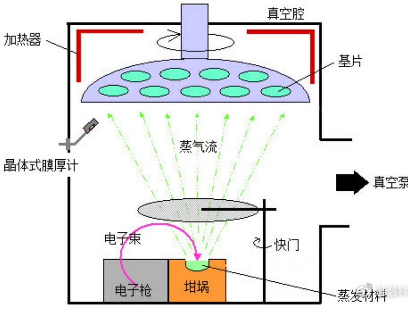
Thermal electrons emitted by the tungsten filament are accelerated and focused by the high-voltage electric field between the cathode and anode, then deflected by a magnetic field to reach the surface of the evaporant material in the crucible. The electron bombardment induces lattice vibration and heat release, melting or subliming the material to complete evaporative deposition.
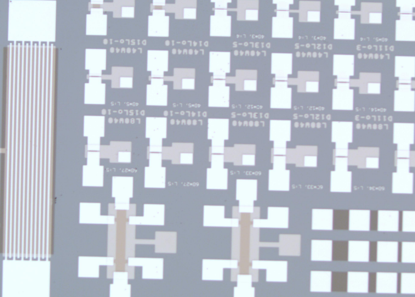
Thin-film transistor devices fabricated with electron-beam evaporated palladium (Pd) thin films.

Address: 800 Dongchuan Road, Minhang District, Shanghai 200240, China
Tel: +86 21 3420 7734
Email: [email protected]







