| Model: | Nanoquest I-XL |
|---|---|
| Function: | Sputtering deposition of high-quality optical and dielectric thin films |
| Engineer: | Fu / +86-21- 34206126-6010 / xuecheng.f@1 |
| Location: | East Area – Thin Film IV |
| Equipment ID: | EFM4IBS01 |
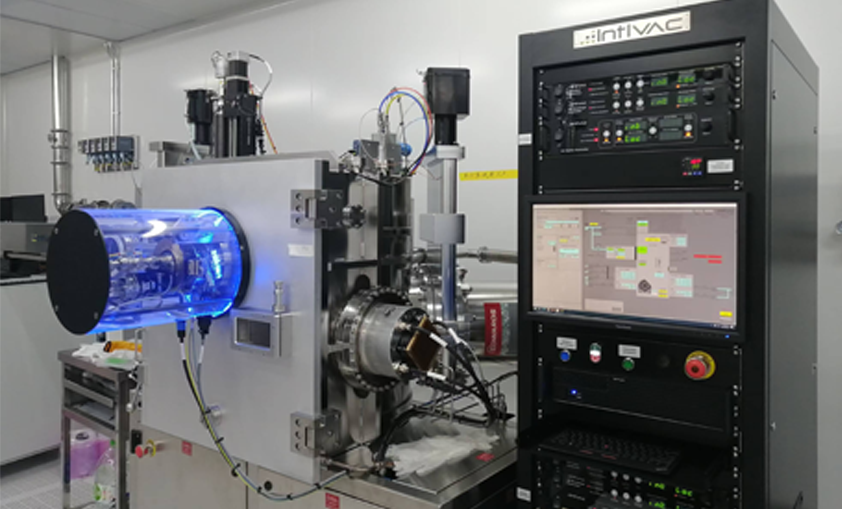
Deposit high-quality optical and dielectric thin films at both room temperature and elevated temperature, including SiO2 , Al2O3 , Ta2O5 , MgF2 and other materials.
Process/Testing Capability
1. Supports reactive sputtering to deposit a variety of oxide and nitride thin films;
2. The substrate stage is heating-enabled with a temperature below 300 °C, suitable for preparing semiconductor thin films by in-situ heating;
3. The angle of the substrate stage is adjustable from 0° to 160°, which meets the hole-filling requirements;
4. Equipped with four targets to realize multilayer film deposition.
Technical Specifications
1. The film thickness uniformity of deposited silicon dioxide is better than ±3% on 6-inch substrates;
2. The film thickness uniformity of deposited aluminum oxide is better than ±2% on 6-inch substrates;
3. Sample processing for sizes under 6 inches is supported, with a sample thickness limited to no more than 2 mm.
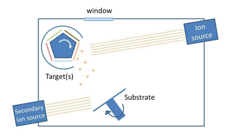
Ion Beam Sputtering (IBSD) is a thin film deposition technology. An ion source is utilized to sputter and deposit target materials (metals or dielectrics) onto the substrate, so as to form metallic or dielectric films. Since the ion beam is monoenergetic (ions possess equal energy) and highly collimated, it enables precise thickness control and the deposition of highly dense, high-quality thin films when compared with other Physical Vapor Deposition (PVD) technologies.

Periodic alternating multilayer films of silicon dioxide and tantalum pentoxide achieve antireflection for light at specific wavelengths.
2.Sample thickness shall not exceed 2 mm.

Address: 800 Dongchuan Road, Minhang District, Shanghai 200240, China
Tel: +86 21 3420 7734
Email: [email protected]







