| Model: | M600 |
|---|---|
| Function: | Capable of depositing high-quality thin films with precisely controllable thickness, including elemental metals, oxide semiconductors and compound materials, at both room temperature and elevated temperature. |
| Engineer: | Fu / +86-21- 34206126-6010 / xuecheng.f@1 |
| Location: | East Area – Thin Film IV |
| Equipment ID: | EFM3MMS01 |
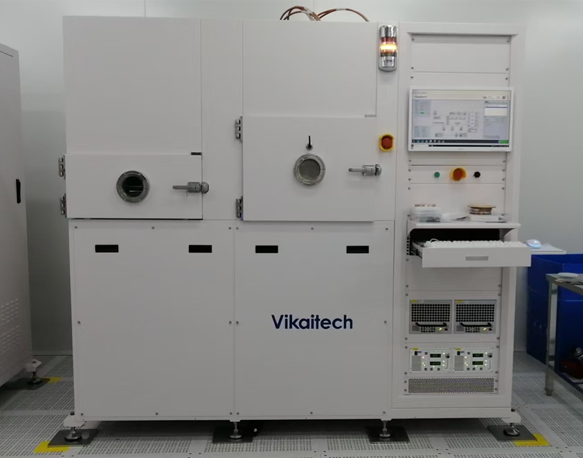
Deposits high‑quality thin films with precisely tunable thickness, covering elemental metals, oxide semiconductors, and compound materials.Available materials include elemental metals, oxides and nitrides such as Cr, Cu, Ni, Al, Ge, Ti, Pt, Ta, SiO2, Mo, W, ITO, and TiNx.
Process/Testing Capability
1. Supports processing of samples smaller than 8 inches with a maximum thickness of 1 cm;
2. Enables reactive sputtering deposition of various oxide and nitride thin films;
3. Equipped with strong magnetic targets for sputtering magnetic materials;
4. Capable of in-situ substrate cleaning, deposition of multi-layer composite films, and co-sputtering composite films with multiple targets;
5. The sample stage supports heating up to 500 °C, suitable for in-situ heated fabrication of semiconductor thin film materials.
Technical Specifications
1. Non-uniformity: ±5% on 8-inch substrates;
2. Sputtering metal gap-fill capability with an aspect ratio of approximately 5:1;
3. Supports sample processing for sizes below 8 inches; maximum sample thickness: 2 mm.
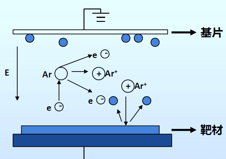
Argon gas is introduced into a high-vacuum environment. After a high-voltage electric field is applied, electrons are accelerated and collide with argon atoms, generating Ar+ ions and additional electrons to form plasma.
Driven by the electric field, Ar+ ions bombard the target surface at high speed, dislodging target atoms and enabling sputtering.

Address: 800 Dongchuan Road, Minhang District, Shanghai 200240, China
Tel: +86 21 3420 7734
Email: [email protected]







