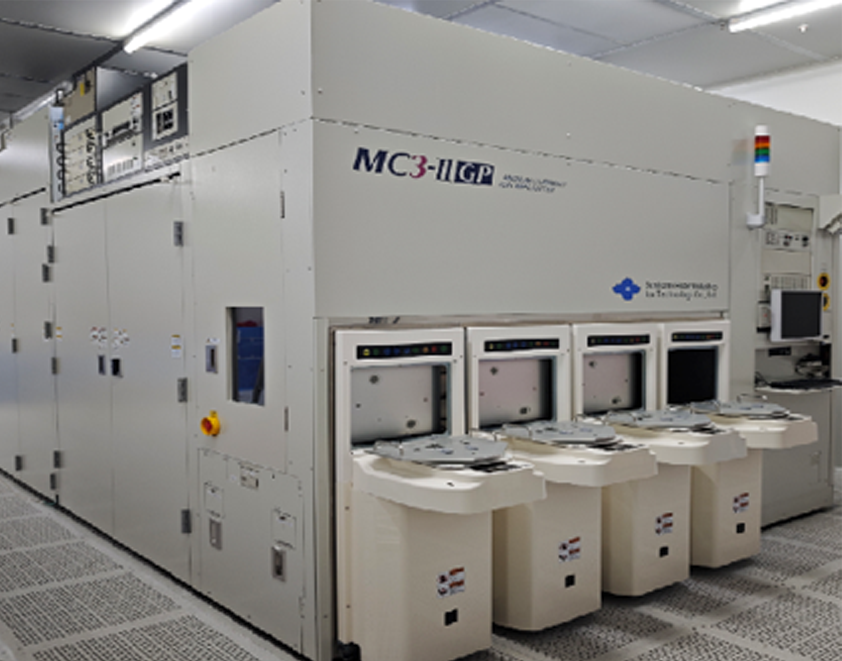
Medium Current Ion Implanter
Operating
Model: MC3-II/GP
Function: Up to 8-inch, 3–960 keV; Implantation available for B, BF₂, P, As, Ar.
Engineer: Li / +86-21- 34206126-6012 / litq@1
Location: East Area – Epitaxy / Ion Implantation
Equipment ID: EEI0MCI01
  • Basic Equipment Information
  • Operating Principle
  • Typical Application Case
Main Applications

It is used for doping semiconductor materials to modify their electrical properties, such as adjusting the threshold voltage, forming shallow junctions/resistors, and fabricating CMOS wells.


Process / Testing Capabilities

Implantation available for B, BF₂, As, P, Ar; Dissociation Energy > 50; Energy Error < 1%; Dose Error < 1%; Angular Error < 0.2°; Repeatability & Uniformity < 0.5%.


Technical Specifications

Dose Range: 1E12 ~ 1E16 atoms/cm²;Tilt Angle Range: 0–60°, Minimum Adjustment Precision: 0.1°;Twist Angle Range: 0–360°, Minimum Adjustment Precision: 0.1°;Beam Parallelism: ≤±0.5°;Wafer Alignment Precision: ≤±0.2°;Temperature: < 100°C;Particle Addition: < 30 ea (≥0.12 μm, 3 mm wafer edge exclusion)

Ion implanters are critical precision equipment in the semiconductor manufacturing process, primarily used to implant ions of specific elements into semiconductor wafers (e.g., silicon wafers), thereby modifying the electrical properties of local wafer regions (e.g., doping concentration, conductivity type, etc.). Their working principle can be summarized into five core steps: ion generation → ion extraction and acceleration → mass analysis and filtration → ion beam transmission and scanning → ion implantation into wafers.

file.name

I. Ion Generation (Ion Source)

Principle: Convert the elements to be implanted (e.g., B, P, As, Ar, etc.) into an ionic state through an ionization process.

Methods: Thermal Ionization: Heat the solid material to cause its evaporation, followed by ionization via electron bombardment.

Gas Ionization: Perform electron bombardment on gaseous substances (e.g., BF₃, PH₃) to ionize gas molecules into corresponding ions (e.g., BF₂⁺, P⁺).


file.name

II. Ion Extraction and Acceleration (Accelerating Electric Field)

Principle: The ions generated by the ion source are extracted and imparted with a specific kinetic energy by means of electric field acceleration.

file.name

III. Mass Analysis and Filtration (Magnetic Analyzer)

Principle: The target ions are screened out by utilizing the principle of magnetic field deflection (e.g., to exclude impurity ions or different isotopes of the same element).

file.name

IV. Ion Beam Transmission and Scanning (Beam Current Control)

Principle: The shape, direction and position of the ion beam are controlled by electromagnetic lenses and scanning systems to ensure its uniform coverage of the entire wafer surface.

file.name

V. Ion Implantation into Wafers (Target Chamber and Wafer Stage)

Principle: The ion beam, after filtration and scanning, ultimately bombards the wafer surface, and the ions penetrate into the wafer interior through kinetic energy deposition to form a doped layer.

file.name

Through the full-process control of ion generation → acceleration → mass filtration → scanning → implantation, the ion implanter achieves precise doping of semiconductor wafers, and it is an irreplaceable key equipment in integrated circuit manufacturing. Its technical challenges lie in high energy precision, high beam current purity, high-uniformity scanning, and the integration of complex vacuum and control systems.

file.name

Boron (B) - Acceptor Impurity (P-type)
  1. Core Doping for PMOS Source/Drain (P⁺ Region) in CMOS Logic Chips: Low-energy ion implantation (e.g., 5~20 keV) forms shallow junctions (<10 nm), used in advanced processes below 7 nm to suppress the short-channel effect.
  2. P-well Formation: High-energy implantation (100~500 keV) creates deep P-wells (junction depth 1~3 μm) in silicon substrates to isolate NMOS devices, with a doping dose of approximately 1e13~1e14 ions/cm².
  3. Threshold Voltage Regulation for NAND Flash Floating Gate Cells in Memory Chips: Boron implantation is used to adjust the threshold voltage distribution of memory cells.
  4. DRAM Channel Doping: Light boron doping (dose ~1e12 ions/cm²) modulates the MOSFET threshold voltage and reduces standby leakage current.

Phosphorus (P) - Donor Impurity (N-type)

  1. NMOS Source/Drain (N⁺ Region): Medium-energy implantation (20~50 keV) forms conductive channels with a doping concentration up to 1e20 cm⁻³, which requires rapid thermal annealing for activation.
  2. Source of Power MOSFETs: High-energy implantation (>100 keV) forms low-resistance N⁺ sources in Si or SiC substrates to reduce on-resistance.
  3. Buried Word Line (WL) in DRAM: Phosphorus diffusion forms N-type buried layers to improve word line conductivity, suitable for high-capacity memory chips (e.g., 14 nm DDR5).
  4. Emitter of Bipolar Junction Transistors (BJTs): Phosphorus diffusion forms N⁺ emitters, which form PN junctions with the base region (boron-doped) and are used in radio frequency (RF) amplification or power switch devices.

Arsenic (As) - Donor Impurity (N-type)

  1. NMOS Source/Drain Extension (SDE) in Advanced Processes: Low-energy implantation (<10 keV) forms ultra-shallow junctions (junction depth <5 nm), used in FinFET/GAA devices below 3 nm to suppress source-drain punch-through.
  2. Buried Layer Doping for High-Speed Logic Chips: Arsenic implantation in silicon substrates forms deep N-type layers (e.g., beneath the buried oxide layer of SOI substrates), used for isolation or conductive layers in RF devices.
  3. Source/Drain of InGaAs Devices: Arsenic implantation in InGaAs substrates forms N⁺ contacts, which utilize its lattice matching with III-V materials to reduce contact resistance (e.g., 5G millimeter-wave chips).

Fluorine (F) - Interface Modulation

  1. FinFET/GAA Gate Engineering: Fluoride ion implantation (energy ~1 keV, dose ~1e14 ions/cm²) beneath metal gates neutralizes interface trap charges and optimizes threshold voltage uniformity (e.g., Intel's 10 nm process).
  2. In addition, BF₂ implantation can be used to achieve ultra-shallow junction implantation of B.
Samples containing metals, powders or liquefiable substances are prohibited. Both front and back sides of the sample must be kept clean. The size of wafer samples shall not exceed 8 inches; small-sized regular samples are processable. 
The list below shows FAQs (click a question to view the answer). If your question is not listed, you can leave a message using the link.
FAQs
  • 01
    Can ultra-high dose implantation (e.g., 1E16 level) be performed?
    The platform uses a medium-current implanter with a wide energy range but moderate beam current. Therefore, a long processing time is required for high-dose implantation conditions. The platform supports a maximum dose of 1E16 level with multiple implantations required. Please confirm specific details with the process engineer.
  • 02
    What is the difference between Tilt angle and Twist angle, and how to apply them?
    Tilt angle refers to the included angle between the ion beam and the wafer's vertical axis, which can be understood as the incident angle (0° for normal incidence). A Tilt angle of 7° is generally used to avoid the channeling effect. Twist angle refers to the counterclockwise rotation angle of the wafer around its center; it is also used to avoid the channeling effect, with a typical setting of 22°.
  • 03
    How to determine ion implantation conditions with known doping concentration and depth?
    Simulation via professional simulation software is required. The platform currently only provides processing services (excluding simulation support).
  • 04
    What information needs to be provided to the process engineer when reserving ion implantation processes?
    1.Sample Information: Whether the sample complies with processing specifications, and whether wafer mounting is required.

    2.Process Condition Information: Parameters including implanted element, energy, dose, angle, etc.

  • 05
    Are other elements supported for implantation besides B, BF₂, P, As, and Ar?
    Only the above elements are supported at present. Implantation of additional elements such as Ge, Si, In, etc., will be gradually developed based on actual demand.
Message Inquiry
If your question is not listed above, please email us at [email protected] or click the button below to submit an inquiry.
Note: "@1" represents "@sjtu.edu.cn"
×