| Model: | Xradia 515 Versa |
|---|---|
| Function: | Enables non-destructive in-situ 3D structural imaging of the sample's internal structure at submicron or micrometer scale, with a spatial resolution of 500 nm. |
| Engineer: | Qu / +86-21- 34207734-8003 / minni.qu@1 |
| Location: | East Area – Testing V |
| Equipment ID: | ETE5XRM01 |
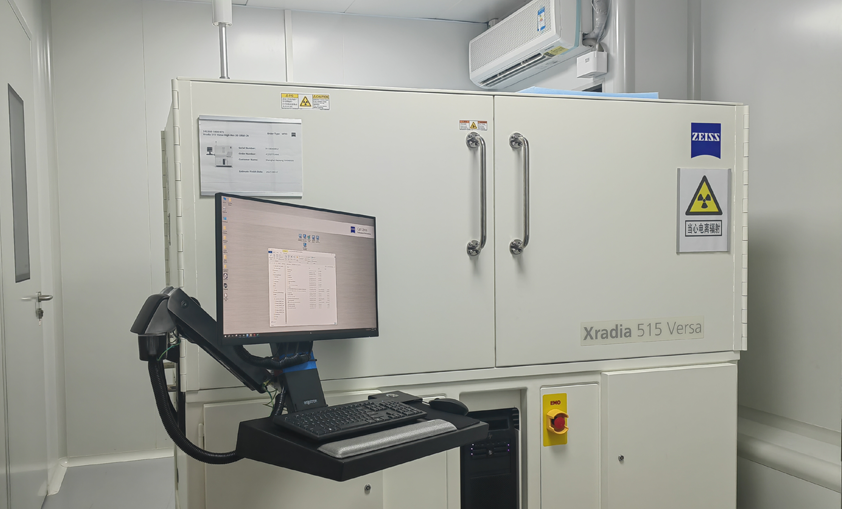
Submicron 3D X-ray Microscope (XRM) with non-destructive 3D tomographic imaging capability. It acquires the internal 3D structure of samples without cutting or staining, and supports virtual slicing and 3D visualization.
Equipped with two-stage magnification technology, it achieves a true spatial resolution of 500 nm. Balancing large sample imaging and multi-scale observation, it enables one-stop inspection from macro to micro scales. The system supports both absorption contrast and phase contrast imaging, making it compatible with a wide range of samples including metals, polymers and biological tissues.
Fitted with precision positioning scanning and dedicated analysis software, it is widely used in scientific research and industrial quality inspection across materials science, energy, microelectronics and life sciences.
Process / Testing Capabilities
Designed for non-destructive 3D imaging of the internal structures of various samples at submicron or micrometer scale, primarily covering semiconductor materials, electronic components, and other composite materials such as high-molecular polymers, coatings and composites.
It works in conjunction with the newly added wafer bonding system, laser ball placement system, TSV deep hole filling electroplating process and other chip structure analysis and testing facilities during the Phase II construction of the platform.
Technical Specifications
Sealed transmission X-ray source; maximum operating voltage ≥ 150 kV, maximum power ≥ 10 W. The sealed transmission X-ray source is movable with a travel range along the X-ray beam axis ≥ 190 mm.Equipped with a CCD detector: pixel count ≥ 2048 × 2048, pixel size ≤ 15 μm. The optically coupled objective lens detector system features no less than 4 magnification objectives (must include 0.4x and 40x objectives).3D field of view (FOV) for 0.4x objective ≥ 50 mm.Spatial resolution for 40x objective better than 0.5 μm.Overall system spatial resolution ≤ 500 nm.Minimum achievable voxel size ≤ 40 nm
It utilizes short-wavelength X-rays to penetrate samples and generates high-resolution projection or tomographic images of microstructures by detecting differences in X-ray absorption, phase shift or scattering. Combining conventional computed tomography (CT) with microscopic magnification technology, it enables non-destructive internal three-dimensional observation. The higher the atomic number and density of a substance, the stronger its X-ray absorption.
3D internal structure observation of semiconductor chips
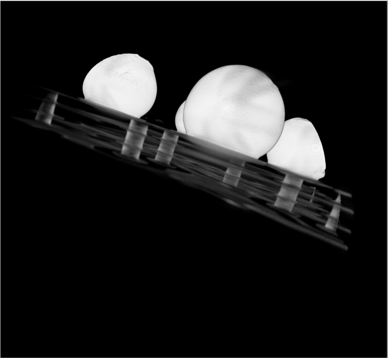
Observation of Cu Filling Quality in TSV Samples
3D morphological observation of jujube pit samples
Maximum sample size: 300 mm. For samples requiring high-resolution testing (voxel resolution ≤ 1 μm), the sample width and thickness should preferably be approximately 1 mm to achieve optimal imaging quality.
Class A equipment
This may be caused by improper coarse alignment. Slightly move the source away from the sample and reduce the pixel size. If the projection is still not visible, return to the Load page to check the sample condition, ensure the sample is securely mounted on the sample stage, re-perform the coarse alignment, and then proceed to the Scout page for settings. If all steps are followed correctly but the projection still does not appear, please contact the equipment administrator.

Address: 800 Dongchuan Road, Minhang District, Shanghai 200240, China
Tel: +86 21 3420 7734
Email: [email protected]







