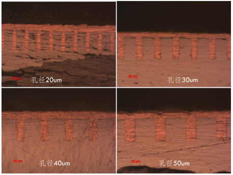
TSV Electroplating Filling Process
Through-Silicon Via (TSV) technology forms vertical electrical interconnections by creating conductive vias through silicon substrates. It is one of the core technologies for stacked-chip interconnection in 3D integrated circuits. High-quality copper filling of deep silicon vias is one of the key process challenges in TSV fabrication. AEMD uses a copper methanesulfonate electroplating system together with advanced additives. By incorporating vacuum-assisted pretreatment and pre-wetting processes, AEMD can achieve void-free, high-fill-ratio bottom-up superfilling for TSV structures with the following capabilities:
Maximum aspect ratio: 10:1
Maximum via depth: 250 μm
Minimum via diameter: 10 μm
Difference Between Conventional Copper Electroplating and TSV Copper Electroplating
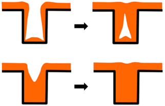
When conventional copper electroplating solutions are used for deep via filling, voids tend to form during the filling process. In TSV electroplating, however, the synergistic effect of specialized additives suppresses copper deposition at the via opening while enhancing deposition at the via bottom. As a result, the deposition rate at the bottom becomes higher than at the top, enabling bottom-up superfilling.
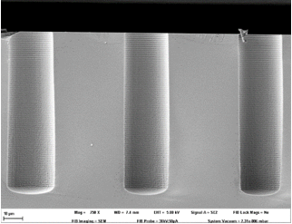
Deep Silicon Vias Fabricated by DRIE
Deep Vias After Electroplating Filling