

AEMD silicon nitride wafers are fabricated using Low-Pressure Chemical Vapor Deposition (LPCVD) in a tube furnace. The available film thickness ranges from 10 nm to 500 nm, with process temperatures above 700°C.
Compared with silicon nitride films deposited by Plasma-Enhanced Chemical Vapor Deposition (PECVD) or sputtering, LPCVD silicon nitride films exhibit:
Higher film density
Better corrosion resistance
Higher hardness
Superior masking performance
For these reasons, LPCVD silicon nitride is widely used as a masking layer for alkaline silicon etching processes.
AEMD’s LPCVD systems employ SVCS horizontal furnace tubes manufactured in the Czech Republic, featuring:
High process stability
Excellent film uniformity
Superior particle control performance
Each silicon nitride furnace tube can process up to 50 wafers per batch, providing excellent within-wafer and wafer-to-wafer uniformity.
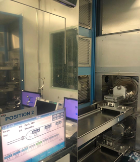
In the semiconductor industry, silicon nitride films are commonly used as:
Dielectric layers
Passivation layers
Hard masks
They are also widely applied in micromechanics and MEMS fabrication.
Definition of active regions during field oxidation processes
Fabrication of membranes, cantilevers, and other MEMS-related mechanical structures
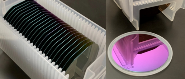
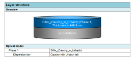
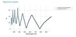
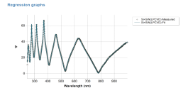
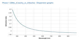
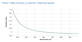
AEMD Silicon Nitride Thin Film Image
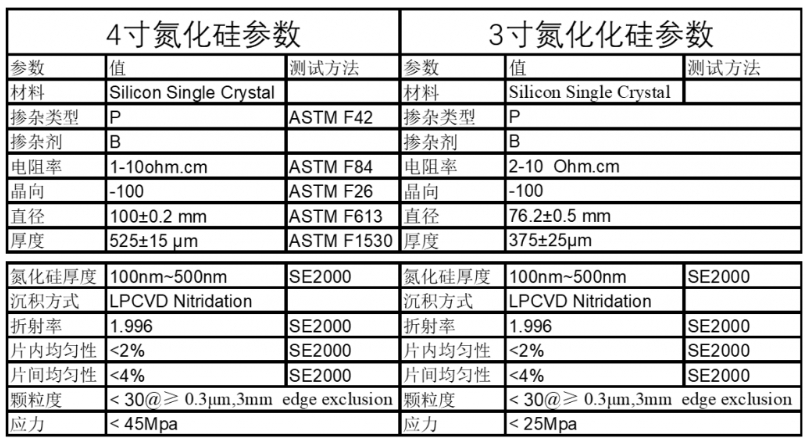
| 类别 | 4寸氮化硅 | 3寸氮化硅 |
| 薄膜结构 | 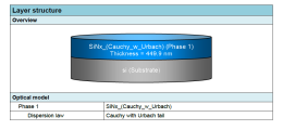 |
 |
|
拟合曲线 |
 |
 |
|
反射率曲线 |
 |
 |






