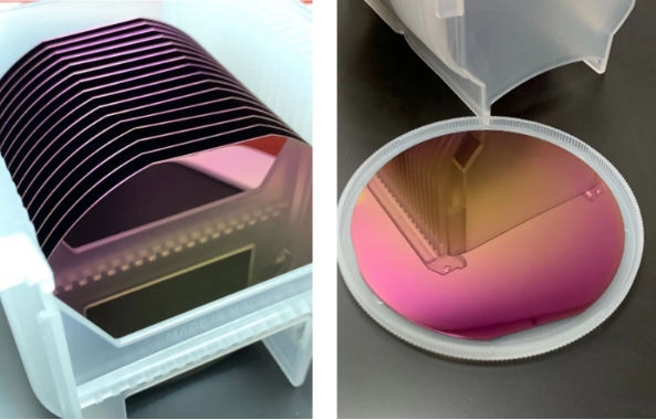
Wet Oxidation Capability: 500 nm – 2 μm
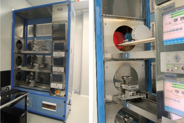
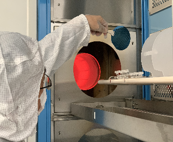
AEMD’s atmospheric oxidation furnaces utilize SVCS horizontal furnace systems manufactured in the Czech Republic, featuring high process stability, excellent film uniformity, and superior particle control performance.
Each oxidation furnace tube can process up to 50 wafers simultaneously while maintaining excellent within-wafer and wafer-to-wafer uniformity.
Thermal oxide layers serve as excellent dielectric insulating materials. In various silicon-based devices, thermally grown oxide layers play critical roles as dopant blocking layers and surface dielectric layers.
1. Ion Implantation Blocking Layer. Silicon dioxide acts as a diffusion mask against impurities. In integrated circuit manufacturing, common dopants such as boron, phosphorus, and arsenic diffuse much more slowly in SiO₂ than in silicon. Therefore, during semiconductor fabrication, an oxide layer is first grown on the silicon wafer surface. After photolithography and development, oxide in selected regions is etched away to form doping windows, allowing selective impurity implantation into designated areas.
2. Gate Oxide Layer. In MOS/CMOS integrated circuit fabrication, SiO₂ is commonly used as the insulating gate dielectric layer of MOS transistors.
3. Dielectric Isolation. Integrated circuit isolation techniques include PN junction isolation and dielectric isolation. Silicon dioxide is widely used for dielectric isolation.
For example, field oxide layers in CMOS processes are used to isolate PMOS and NMOS transistors and their active regions.
4. Insulating Dielectric Layer. Silicon dioxide is an excellent electrical insulator. In multilayer metal interconnect structures, it serves as the insulating dielectric between upper and lower metal layers to prevent short circuits.
5. Metal Wire Bonding Testing. Thermal oxide layers are also used in metal wire bonding and related testing applications.
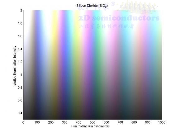
AEMD provides silicon oxide wafers fabricated using both dry and wet oxidation processes with various process parameters available.
The products feature competitive pricing and convenient procurement.
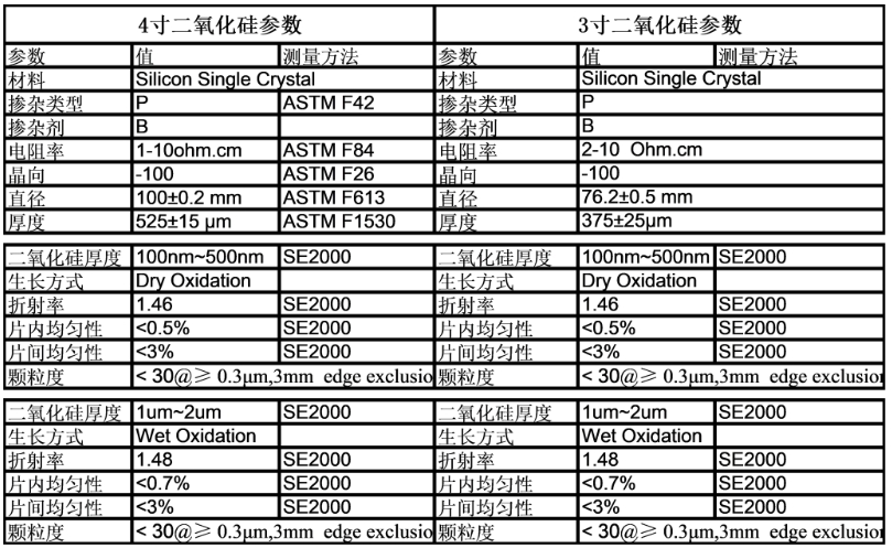
| 类别 |
4寸二氧化硅 |
3寸二氧化硅 |
| 薄膜结构 | 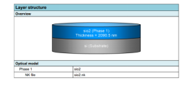 |
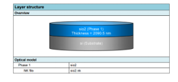 |
|
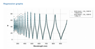
拟合曲线 |
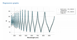 |
 |
|
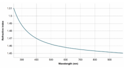
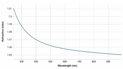
反射率曲线 |
 |
 |