

TEM sample support membranes
X-ray observation windows
Chemically inert and high-temperature-resistant substrates for in-situ sample processing and subsequent observation
Vacuum isolation windows/chambers
Nanopore DNA sequencing
High chemical stability
High mechanical strength
Excellent X-ray transparency
Capable of withstanding temperatures up to 1000°C
High surface flatness (surface roughness < 1 nm)
Excellent hydrophilicity after plasma treatment
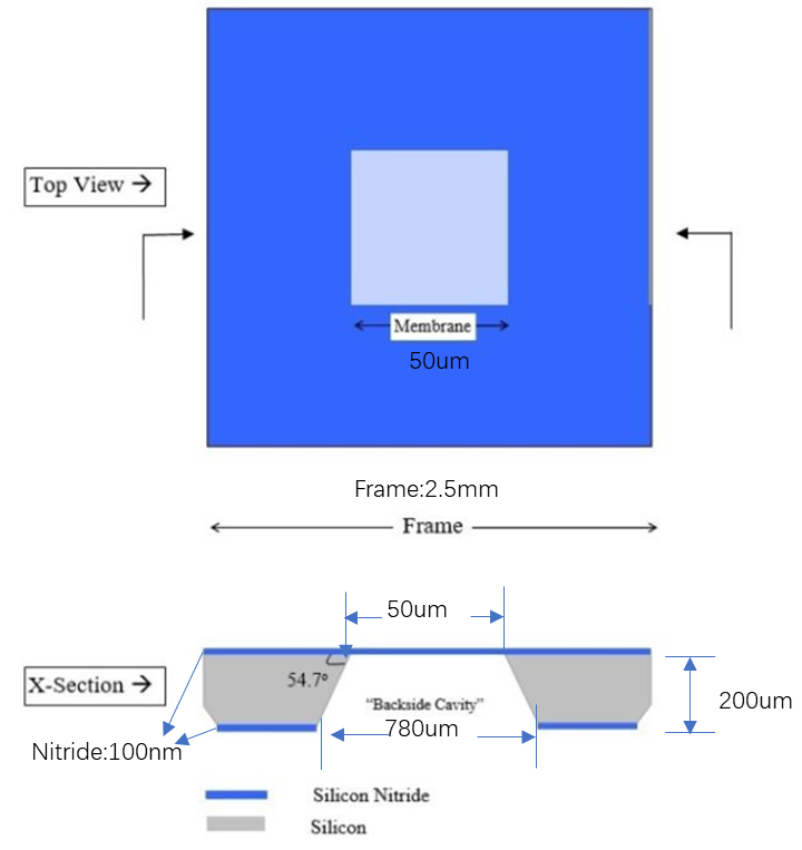
Deposition Method: Low-stress LPCVD furnace depositionSilicon Nitride Film Thickness: 100 nm
Membrane Stress Level: <100 MPa (tensile)
Refractive Index: 2.2 ± 0.05
Window Size: 52 × 52 μm
Frame Thickness: 200 μm
Outer Dimensions: 2.5 × 2.5 mm
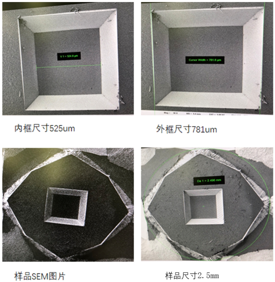
Silicon nitride membrane windows can be fabricated on substrates with different crystal orientations, including (100), (110), and (111).
Users may request customization based on:
Substrate thicknesses ranging from 200 μm to 600 μm
Silicon nitride film thicknesses ranging from 20 nm to 200 nm
Different window sizes such as 30 × 30 μm, 50 × 50 μm, and 100 × 100 μm
Low-stress silicon nitride TEM windows can also be processed using FIB drilling to create nanopores with diameters of 50 nm or larger.
For additional requirements, please contact the process engineer.






