

The AEMD platform employs internationally advanced micro/nanofabrication technologies. Based on mature processes such as lithography and dry etching, it is capable of achieving sidewall etching with tunable inclination angles and smooth surface morphology.
Inclined-angle insulating dielectric layers for improved sidewall coverage
Three-dimensional surface structures in the optical industry, such as microlenses, microgrooves, microcones, and microprisms
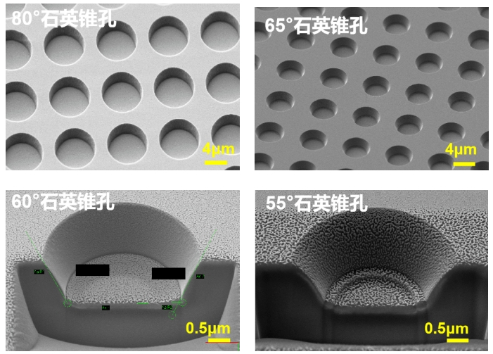
The etched surface quality is high, with post-etch surface quality comparable to the pre-etch condition.
The minimum feature size of the pattern can reach 5 μm.
Etching materials include bulk quartz and silicon oxide thin films.
Processing area: up to 6-inch wafers, with compatibility for diced samples.
The platform also provides customized services. Based on customer application conditions and environmental parameters, cone/truncated-cone etching processes can be designed. For detailed requirements, please contact the process engineers for consultation.






