

The AEMD platform employs internationally advanced micro/nanofabrication technologies. Based on mature processes such as thermal reflow and dry etching, it develops and produces high-quality microlens arrays.
copiers, image scanners, fax machines, and cameras;
medical and healthcare devices.
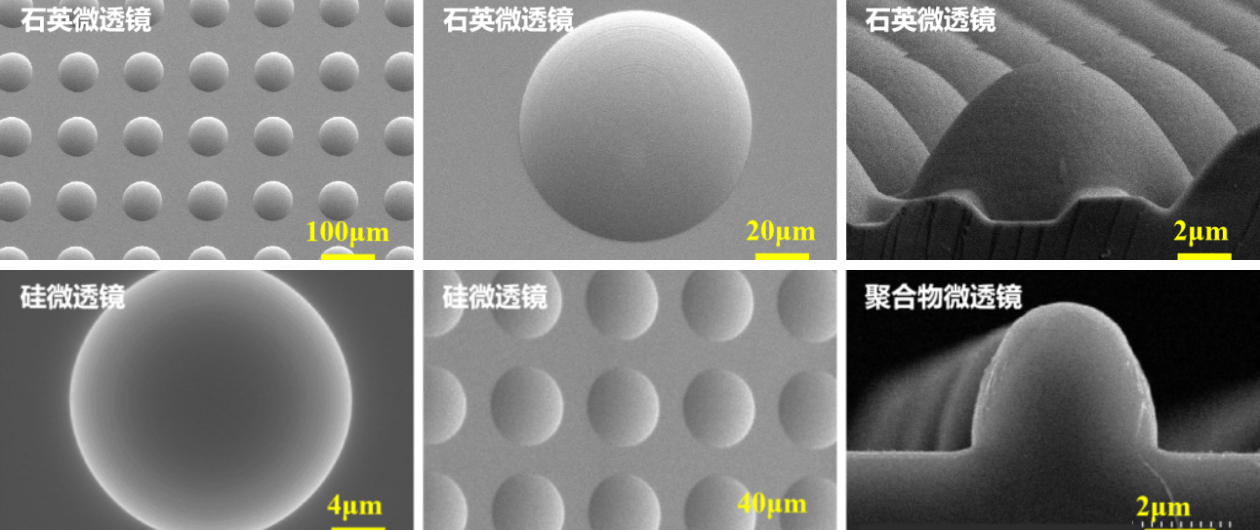
Lens shapes can be circular, square, hexagonal, or other user-defined geometries.
Lens materials include quartz, silicon, polymers, and photoresists.
Substrate materials can be glass, silicon, quartz, metals, or integrated circuit wafers.
Processing area: up to 6-inch wafers, with compatibility for diced samples.
The platform also provides customized services. Based on customer application conditions and environmental parameters, various microlens arrays with tailored materials and design specifications can be developed. For detailed requirements, please contact the process engineers for consultation.






