| Model: | LKJ-ID-150 |
|---|---|
| Function: | 1. RIE etching of metal thin films such as Al, Ni, Cr and Ti; 2. Polysilicon etching; 3. Etching of III-V group semiconductors. |
| Engineer: | Mao / +86-21- 34206126-6009 / maohaiping@1 |
| Location: | West Area – Thin Film IA |
| Equipment ID: | EMCAIBE01 |
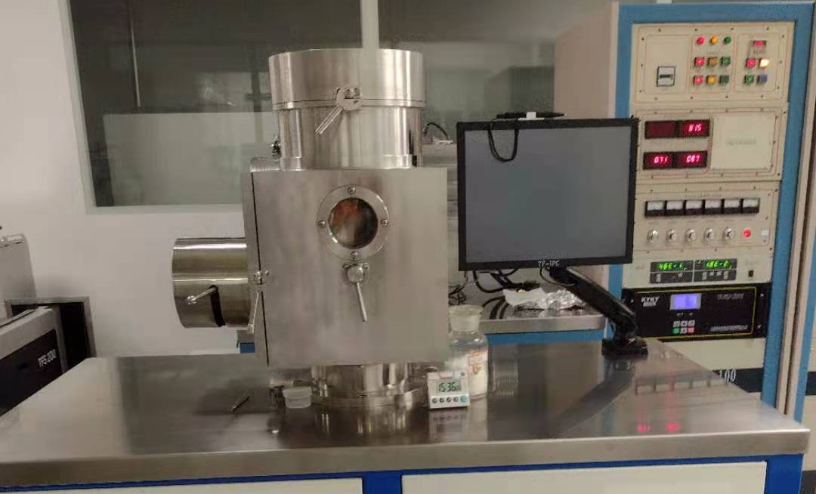
This equipment etches the substrate surface by utilizing low-energy parallel Ar⁺ ion beams. Adopting a pure physical etching principle, it delivers high resolution and excellent sidewall verticality. It is capable of etching nearly all types of materials, including metals, alloys, oxides, compound semiconductors and more.
Process / Testing Capabilities
1. Etching uniformity and repeatability: the uniformity of 4-inch substrates is better than ±5%, and the repeatability is better than ±5%;
2. Capable of ion beam cleaning and ultimate surface polishing of materials.
Technical Specifications
1. Aperture of LKJ-series ion source: Φ150 mm;
2. Adjustable ion energy range: 0~1000 eV;
3. Recommended applicable ion energy: 0~750 eV;
4. Peak beam current: ≥130 mA;
5. Recommended operating beam current: 0~100 mA;
6. Water-cooled stage temperature:-5℃~25℃;Workpiece stage diameter: Ф150mm;
7. Rotation speed: 9 RPM; Maximum substrate size: ≤4 inches.
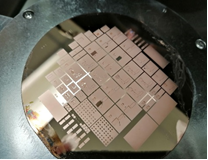
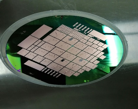
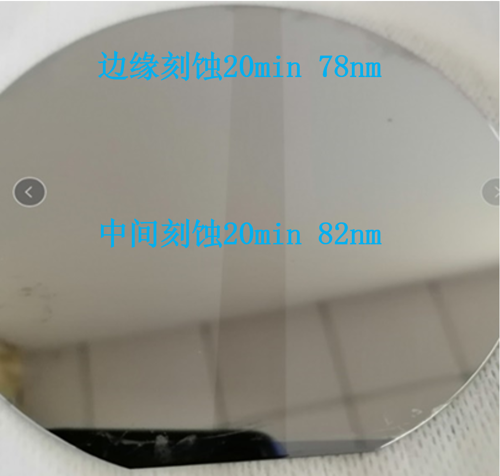
2. The gold-plated quartz wafers for sensor fabrication were etched by the ion beam etching system, with an average etching rate of 4 nm/min and a center-to-edge non-uniformity of approximately 5%, which fully meets experimental requirements.

Address: 800 Dongchuan Road, Minhang District, Shanghai 200240, China
Tel: +86 21 3420 7734
Email: [email protected]







