| Model: | SM-200 |
|---|---|
| Function: | Primarily used for the spin coating process in photolithography; enables uniform coating of photoresist or other liquid materials, suitable for high-precision coating on wafers and substrates. |
| Engineer: | Zhang / +86-21-34206126-6029 / captianzhangdi@1 |
| Location: | East Area – Lithography IIIA |
| Equipment ID: | EDD2SMS01 |
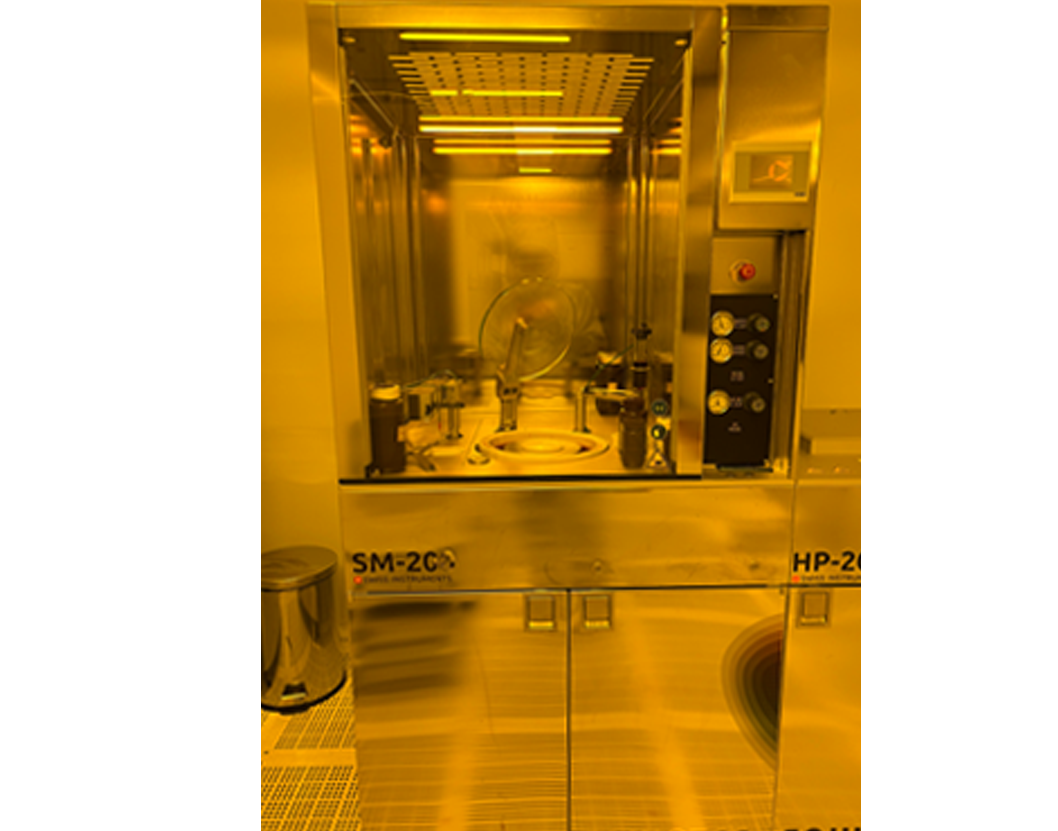
1. Mainly used for spin coating in photolithography processes;
2. Capable of uniformly coating photoresist, electron beam resist, bio-coatings, or other functional liquid materials;
3. Suitable for high-uniformity coating of wafers (1–8 inches) and special substrates.
Process / Testing Capabilities
1. Compatible with 1–8 inch wafers, supports multiple size configurations;
2. Equipped with automatic spin coating, automatic/manual dispensing, and manual loading/unloading;
3. Adjustable process parameters: spin speed, acceleration, time, and rotation direction;
4. Supports coating uniformity testing, edge bead removal (EBR), and backside rinse verification.
Technical Specifications
1. Supports spin coating for wafers of 1/2/3/4/5/6/7/8 inches;
2. Manual wafer loading/unloading; automatic dispensing (switchable to manual),automatic spin coating;
3. Spin speed range: 0–6000 rpm; acceleration reaches 6000 rpm within 0.6 seconds;
4. Speed control accuracy: ±1 rpm; rotation direction: clockwise and counterclockwise;
5. Supports edge bead removal (EBR) and backside rinse functions.
Used in photolithography spin coating processes to uniformly apply photoresist or other liquid materials, enabling high-precision coating on wafers and substrates.
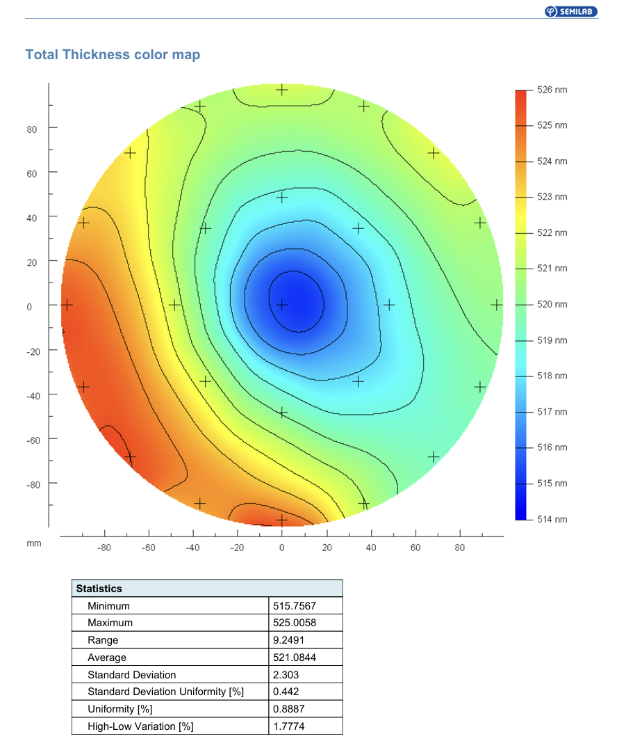
1. Samples must be confirmed with process engineers in advance
2. Both frontside and backside of the samples must be flat and clean
Available all day. The sample must be confirmed with the process instructor in advance. Both the front and back surfaces of the sample must remain flat and clean. Do not touch the sample directly with your hands before use.
The waste liquid container needs to be replaced

Address: 800 Dongchuan Road, Minhang District, Shanghai 200240, China
Tel: +86 21 3420 7734
Email: [email protected]







