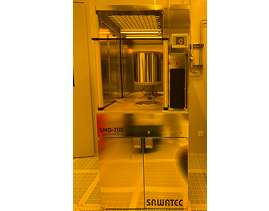
| Model: | SMD-200 |
|---|---|
| Function: | Primarily used in the photolithography development process. Utilizes spray development technology to ensure uniform development, suitable for high-precision microelectronics and semiconductor manufacturing. |
| Engineer: | Zhang / +86-21- 34206126-6029 / captianzhangdi@1 |
| Location: | East Area – Lithography IIIA |
| Equipment ID: | EDD2SMD01 |
1. Used for photoresist pattern development processes;
2. Supports multiple development methods, including spray development, immersion development, and flow rinse;
3. Widely applied in high-precision pattern transfer processes for IC manufacturing, MEMS fabrication, optoelectronics, and sensors.
1. Supports development processes for wafers of 2–8 inches;
2. Programmable with up to 20 development steps for complex process flows;
3. Supports high-speed rotational development (0–3000 rpm);
4. Development head supports spray, immersion, and flow modes; robotic arm enables automatic reciprocating motion;
5. Supports post-development nitrogen drying, spin drying, and backside rinse.
1. Compatible with 2/3/4/5/6/7/8 inch wafers;
2. Supports up to 20 programmable steps;
3. Spin speed range: 0–3000 rpm; acceleration reaches 6000 rpm within 0.3 seconds;
4. Supports multiple development modes: robotic arm movement, immersion, flow, and spray;
5. Supports nitrogen drying, spin drying, and backside rinse.
The Sawatec SMD-200 employs spray development technology, where the developer is precisely sprayed to uniformly cover the photoresist surface, dissolving and removing either exposed or unexposed regions depending on the process. Combined with rotational control and liquid flow regulation, the system ensures uniform development and enhances process precision in microelectronics and semiconductor manufacturing.
1. Samples must be confirmed with process engineers in advance;
2. Both frontside and backside of the samples must be flat and clean.
Available for use throughout the day. Samples must be confirmed with process engineers in advance. Both frontside and backside of the samples must be flat and clean. Please keep the equipment clean and tidy after use.
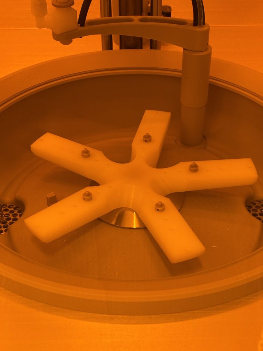
Remove the knob, adjust it according to the wafer size, and reinstall it accordingly

Address: 800 Dongchuan Road, Minhang District, Shanghai 200240, China
Tel: +86 21 3420 7734
Email: [email protected]







