| Model: | SI 500 |
|---|---|
| Function: | This equipment is used for the etching of compound semiconductor materials, including GaAs-based, InP-based and GaN-based materials. |
| Engineer: | Liu / +86-21- 34206126-6013 / minliu@1 |
| Location: | East Area – Compound Semiconductor |
| Equipment ID: | ECS0CSE01 |
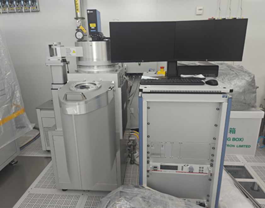
It is mainly used for etching various compound semiconductor materials, and is widely applied to the manufacturing and processing of communication, optical communication, radio frequency devices and other components.
Process / Testing Capabilities
It supports a maximum 8-inch substrate and is backward compatible with various small-size wafers and fragmented samples.
Technical Specifications
Etching rate of GaAs-based materials>400 nm/min with verticality of 88–92°;Controllable etching rate for GaN ranging from 1–5 nm/min;Etching rate of InP>300 nm/min with verticality of 88–92°.

Address: 800 Dongchuan Road, Minhang District, Shanghai 200240, China
Tel: +86 21 3420 7734
Email: [email protected]







