| Model: | µGALV |
|---|---|
| Function: | Electroplating filling of high aspect ratio structures including silicon blind vias, silicon through vias, glass blind vias and glass through vias |
| Engineer: | Tian / +86-21- 34206126-6031 / miaotian@1 |
| Location: | East Area – Electroplating |
| Equipment ID: | EPL0TSV01 |
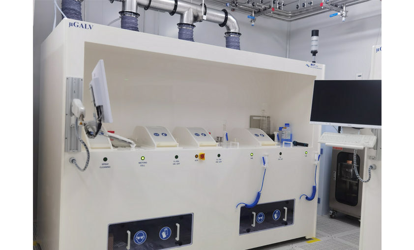
Electroplating fills high aspect ratio structures including silicon blind vias, silicon through vias, glass blind vias and glass through vias. Only metallic copper can be deposited. The filling effect differs depending on aspect ratio and aperture diameter.
This is a process of depositing copper layers on the substrate surface by electrochemical means. The electroplating solution consists of copper sulfate, conductive salts, pH regulators and other components. During electroplating, the substrate acts as the cathode. After power-on, copper ions are reduced and precipitated on the cathode surface to form a copper coating.
Filling effect of deep vias with an aspect ratio of 10:1
At least 200 nm to ensure continuity within the vias.

Address: 800 Dongchuan Road, Minhang District, Shanghai 200240, China
Tel: +86 21 3420 7734
Email: [email protected]







