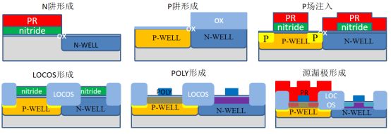
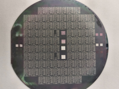
The platform provides customized 4–8 inch wafer fabrication for dual-well, dual-metal CMOS chips, and also supports modular CMOS process development and validation, including shallow trench isolation (STI) technology validation, source/drain engineering, strain engineering, contact hole technology, and metal interconnects.
Schematic of CMOS device simulation and fabrication flow